Dry Etching
1. High Anisotropy & Precision Control: Enables vertical sidewalls and accurate critical dimension (CD) control for sub-micron structures.
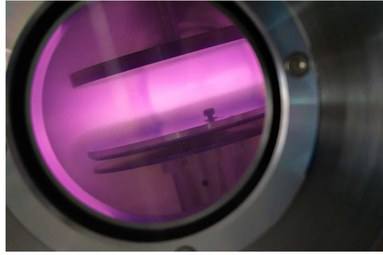
2. Plasma-Based Material Selectivity: Supports selective etching of silicon, SiO₂, Si₃N₄, metals, compound semiconductors, and dielectric films.
3. Advanced RF Power & Gas Flow Control: Precise management of plasma density, pressure, and gas chemistry for consistent repeatability.
4. Endpoint Detection Systems: Optical emission spectroscopy (OES) or interferometry for real-time etch stop control.
5. Automation & Cleanroom Compatibility: Cassette-to-cassette wafer handling, recipe management, SECS/GEM integration, and low particle design.
DESCRIPTION
Dry etching equipment is a critical semiconductor manufacturing system used to selectively remove material from a wafer surface using plasma-based or reactive ion processes. Unlike wet etching, dry etching uses ionized gases (plasma) under vacuum conditions to achieve highly anisotropic, precise material removal, enabling fine pattern transfer in both front-end and back-end semiconductor processes. Dry etching plays a vital role in defining transistor gates, contact holes, vias, interconnect structures, MEMS features, and advanced packaging layers, supporting today’s high-density and high-performance chip architectures.
Types of Dry Etching Systems-
1. Reactive Ion Etching (RIE) Systems
2. Inductively Coupled Plasma (ICP) Etchers
3. Deep Reactive Ion Etching (DRIE) Systems
4. Plasma Ashing / Descum Systems
5. High-Density Plasma (HDP) Etchers