1. Precision Pattern Exposure: Uses UV, deep-UV (DUV), or other wavelength light sources with high-resolution optics to accurately project circuit patterns onto wafer surfaces with tight overlay and alignment control.
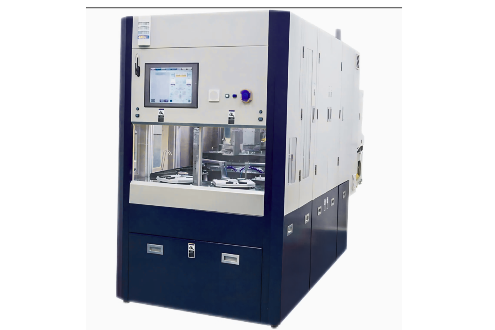
2. Stepper/Scanner Architecture: Step-and-repeat or step-and-scan motion delivers high throughput while maintaining excellent image fidelity and resolution across the wafer.
3. Advanced Optics & Alignment: Integrated alignment systems and interferometric controls ensure precise registration between layers during multi-layer patterning.
4. Support for Multiple Nodes: Equipment spans technologies from legacy i-line and KrF systems for larger geometries to immersion and multi-patterning capable DUV tools for finer features.
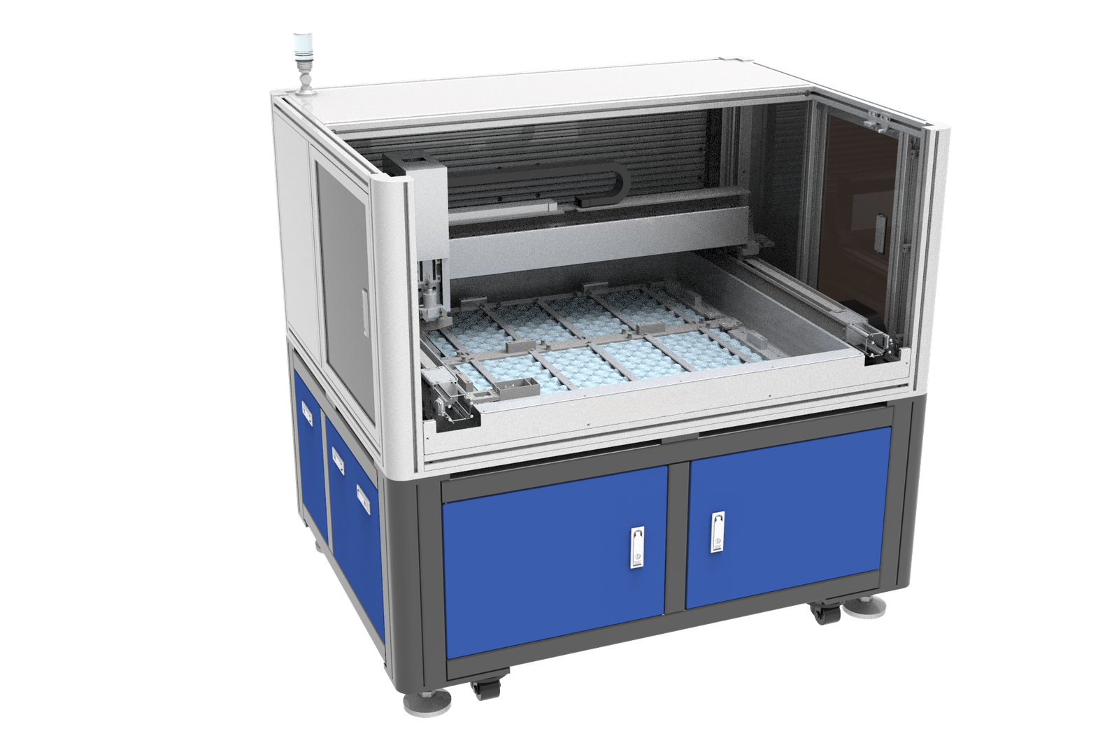
5. Automation & Metrology Integration: Modern systems include wafer handling automation and feedback metrology for real-time correction and yield optimization.